Compact Power: The Billion-Dollar Bet on Advanced Chip Packaging
As chip miniaturization hits its limits, is the rush toward advanced packaging brilliance or just a billion-dollar band-aid?
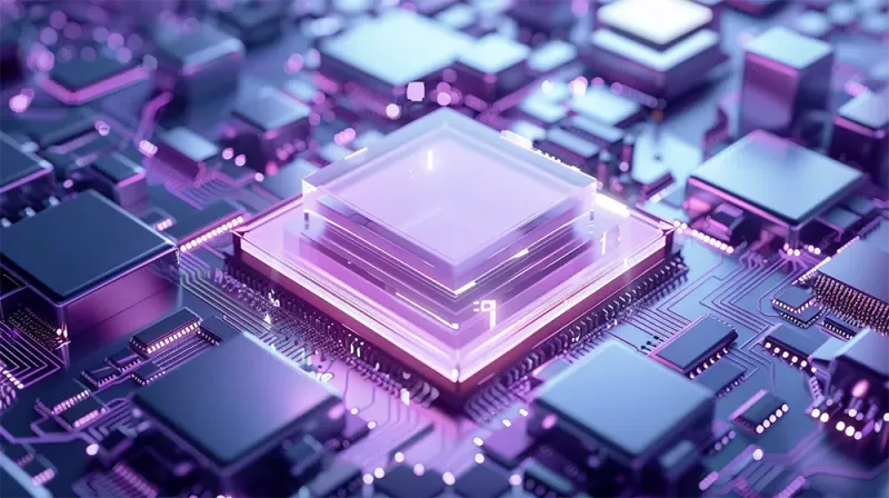
The race to boost semiconductor performance as miniaturization plateaus has led giants like Samsung and Nvidia towards 'advanced packaging'. This technique integrates multiple chips into compact assemblies, enhancing speed and efficiency dramatically.
Samsung's recent $40 billion investment into a Texas facility underscores this shift, aiming to enhance AI chip production on U.S. soil. Advanced packaging, such as High Bandwidth Memory (HBM) and Chip-on-Wafer-on-Substrate (CoWoS), allows for closer component integration, pushing past previous technological boundaries.
This strategic pivot not only meets rising AI demands but also redefines industry collaborations, suggesting a future where chip performance and innovation are bound by assembly finesse rather than mere transistor size.
Read the full article on Financial Times.
----
💡 We're entering a world where intelligence is synthetic, reality is augmented, and the rules are being rewritten in front of our eyes.
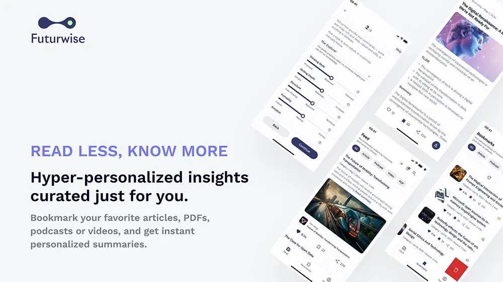
Staying up-to-date in a fast-changing world is vital. That is why I have launched Futurwise; a personalized AI platform that transforms information chaos into strategic clarity. With one click, users can bookmark and summarize any article, report, or video in seconds, tailored to their tone, interests, and language. Visit Futurwise.com to get started for free!

Dr Mark van Rijmenam
Dr. Mark van Rijmenam, widely known as The Digital Speaker, isn’t just a #1-ranked global futurist; he’s an Architect of Tomorrow who fuses visionary ideas with real-world ROI. As a global keynote speaker, Global Speaking Fellow, recognized Global Guru Futurist, and 5-time author, he ignites Fortune 500 leaders and governments worldwide to harness emerging tech for tangible growth.
Recognized by Salesforce as one of 16 must-know AI influencers , Dr. Mark brings a balanced, optimistic-dystopian edge to his insights—pushing boundaries without losing sight of ethical innovation. From pioneering the use of a digital twin to spearheading his next-gen media platform Futurwise, he doesn’t just talk about AI and the future—he lives it, inspiring audiences to take bold action. You can reach his digital twin via WhatsApp at: +1 (830) 463-6967.